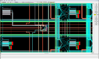
 FPGA Design
The know-how of Asic and FPGA design covers many application fields: implementation of SDH/ATM and
FPGA Design
The know-how of Asic and FPGA design covers many application fields: implementation of SDH/ATM and packet technologies, realization of FPGAs that can manage tens of Giga of traffic, implementation of digital
circuitry for RF/wireless solutions, transport of different protocols on emerging tecnology as CES/SATOP or
GFP. The team has a proven and long term experience in FPGA design with the main device vendors (Altera,
Lattice, Xilinx), knowledge of the main software development tools and design work flows and mainly it has
the capability to deal with all issues related to the introduction of the
latest technologies, to define the system level functional and
behavioural specifications, not limited to the pure hardware
implementation aspects.
The FPGA design is fully integrated with the hardware and RF design,
giving to the card design process a specific analysis and syntesis
capability in order to
determine the best
solution, in compliance
with the target costs,
the foreseen time to
market and the flexibility and modularity expectations.
The team has also the capability to perform board simulation
for verification of schematics.
The FPGA design is also supported for test and verification by
the FW team.
packet technologies, realization of FPGAs that can manage tens of Giga of traffic, implementation of digital
circuitry for RF/wireless solutions, transport of different protocols on emerging tecnology as CES/SATOP or
GFP. The team has a proven and long term experience in FPGA design with the main device vendors (Altera,
Lattice, Xilinx), knowledge of the main software development tools and design work flows and mainly it has
the capability to deal with all issues related to the introduction of the
latest technologies, to define the system level functional and
behavioural specifications, not limited to the pure hardware
implementation aspects.
The FPGA design is fully integrated with the hardware and RF design,
giving to the card design process a specific analysis and syntesis
capability in order to
determine the best
solution, in compliance
with the target costs,
the foreseen time to
market and the flexibility and modularity expectations.
The team has also the capability to perform board simulation
for verification of schematics.
The FPGA design is also supported for test and verification by
the FW team.


 © 2011-2014 BTP research All rights reserved
PRIVACY
LOG IN
© 2011-2014 BTP research All rights reserved
PRIVACY
LOG IN

 “inspiring partners
for
finding solutions”
THE COMPANY
OUR SERVICES
OUR GROUP
“inspiring partners
for
finding solutions”
THE COMPANY
OUR SERVICES
OUR GROUP
 Power
Our capability
RF design
OUR SERVICES
IP Solutions
FW/SW
Hardware design
FPGA design
DISCLAIMER
EMAIL FROM/TO
Power
Our capability
RF design
OUR SERVICES
IP Solutions
FW/SW
Hardware design
FPGA design
DISCLAIMER
EMAIL FROM/TO